
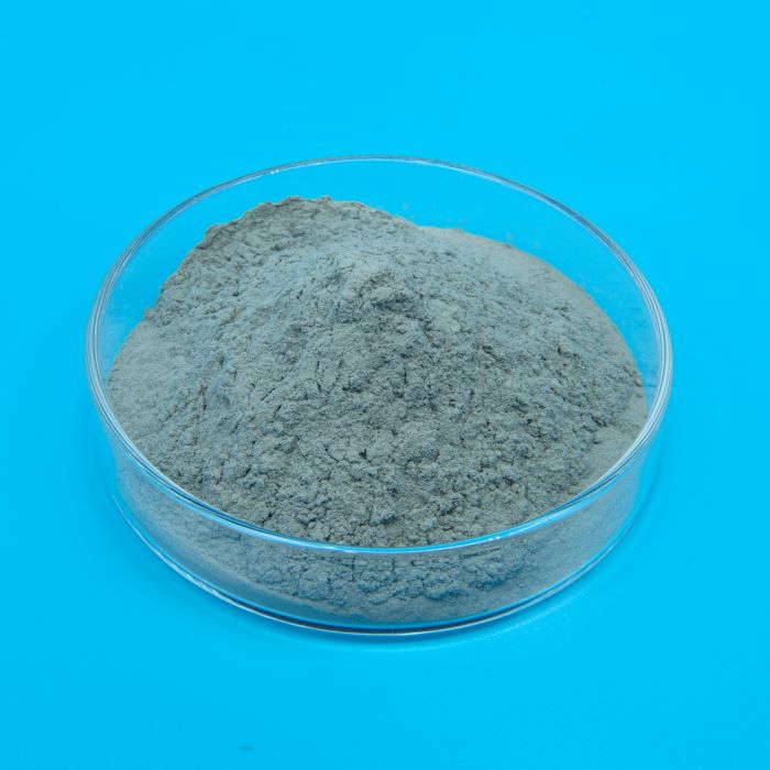

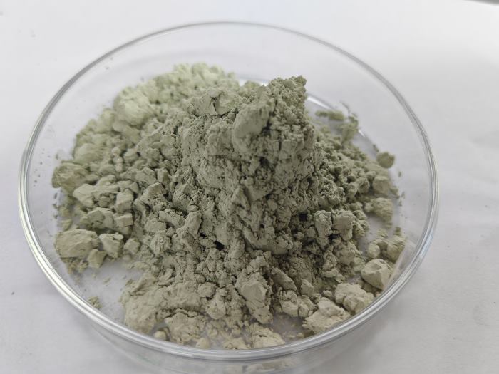
Green Silicon Carbide 1200# for Glass Wafer Grinding and Polishing
Green Silicon Carbide (GC) 1200# powder is a high-purity precision abrasive specially developed for grinding, fine lapping and pre-polishing of glass wafers, optical glass substrates and related semiconductor optical components. It adopts advanced crushing, acid pickling and strict narrow particle size classification processes to guarantee stable and consistent abrasive performance for high-end semiconductor manufacturing.
GC powder features high hardness, sharp cutting edges and moderate self-sharpening property. During wafer processing, grains fracture along the cleavage plane to continuously generate new cutting edges, maintaining steady material removal rate without rapid passivation. Its excellent thermal conductivity effectively dissipates frictional heat generated in grinding, reducing thermal deformation, chipping, edge collapse and subsurface microcracks on thin glass wafers. Low thermal expansion ensures superior form retention for delicate structures such as V-groove substrates and optical cover plates, which are widely adopted in semiconductor packaging, optical communication and optoelectronic modules.
Strict impurity control is a core advantage of this grade. Low iron content and minimal magnetic foreign matters avoid contamination, stains and scattering defects on optical surfaces. The tightly controlled particle size distribution greatly lowers the risk of deep scratches, delivering uniform fine texture and shallow damage layer after fine grinding. It creates an ideal surface foundation for subsequent cerium oxide final polishing, helping reduce polishing workload and improve yield in mass semiconductor production.
Compared with black silicon carbide, green silicon carbide has higher purity and better chemical inertness. Unlike alumina abrasives with poor self-sharpening, GC 1200# balances cutting capacity and surface quality well. It is widely used for fine grinding of glass wafers used in optical transceiver chips, image sensor covers, wafer-level optics and semiconductor light guide components.
Suitable for batch lapping machines and precision surface grinders, this 1200# green silicon carbide powder supports stable, repeatable processing. It helps manufacturers achieve required roughness, profile accuracy and low surface defect rate, serving as a reliable cost-effective abrasive solution for semiconductor glass wafer processing.
TYPICAL CHEMICAL ANALISIS [%]
| SiC | Fe2O3 | F.C | F.Si | SiO2 | LOI |
| 98.0-99.5 | ≤0.15 | ≤0.30 | ≤0.40 | ≤0.70 | < 0.09 |
PARTICLE SIZE DISTRIBUTION
CHAPTER Ⅰ(JIS STANDARD)
| Size | DO(um) | D3(um) | D50(um) | D94(um) |
| #240 | ≤127 | ≤103 | 57.0±3.0 | ≥40 |
| #280 | ≤112 | ≤87 | 48.0±3.0 | ≥33 |
| #320 | ≤98 | ≤74 | 40.0±2.5 | ≥27 |
| #360 | ≤86 | ≤66 | 35.0±2.0 | ≥23 |
| #400 | ≤75 | ≤58 | 30.0±2.0 | ≥20 |
| #500 | ≤63 | ≤50 | 25.0±2.0 | ≥16 |
| #600 | ≤53 | ≤41 | 20.0±1.5 | ≥13 |
| #700 | ≤45 | ≤37 | 17.0±1.5 | ≥11 |
| #800 | ≤38 | ≤31 | 14.0±1.0 | ≥9.0 |
| #1000 | ≤32 | ≤27 | 11.5±1.0 | ≥7.0 |
| #1200 | ≤27 | ≤23 | 9.5±0.8 | ≥5.5 |
| #1500 | ≤23 | ≤20 | 8.0±0.6 | ≥4.5 |
| #2000 | ≤19 | ≤17 | 6.7±0.6 | ≥4.0 |
| #2500 | ≤16 | ≤14 | 5.5±0.5 | ≥3.0 |
| #3000 | ≤13 | ≤11 | 4.0±0.5 | ≥2.0 |
| #4000 | ≤11 | ≤8.0 | 3.0±0.4 | ≥1.8 |
| #6000 | ≤8.0 | ≤5.0 | 2.0±0.4 | ≥0.8 |
| #8000 | ≤6.0 | ≤3.5 | 1.2±0.3 | ≥0.6 |
CHAPTER Ⅱ(FEPA STANDARD)
| Size | D3(um) | D50(um) | D94(um) |
| F230 | <82 | 53.0±3.0 | >34 |
| F240 | <70 | 44.5±2.0 | >28 |
| F280 | <59 | 36.5±1.5 | >22 |
| F320 | <49 | 29.2±1.5 | >16.5 |
| F360 | <40 | 22.8±1.5 | >12 |
| F400 | <32 | 17.3±1.0 | >8 |
| F500 | <25 | 12.8±1.0 | >5 |
| F600 | <19 | 9.3±1.0 | >3 |
| F800 | <14 | 6.5±1.0 | >2 |
| F1000 | <10 | 4.5±0.8 | >1 |
| F1200 | <7 | 3.0±0.5 | >1(at 80%) |
| F1500 | <5 | 2.0±0.4 | >0.8(at 80%) |
| F2000 | <3.5 | 1.2±0.3 | >0.5(at 80%) |
Mainly Applications
-Bonded Abrasives and Coated abrasives
-Blasting,surface Treatment,Rust Removal
-Wet and dry blast media,grinding and polishing etc
-Floor/Wall laminates,Wear-resistant
-Ceramic products: Ceramic and Tiles,Ceramic filter plate,ceramic membrane etc
-Teflon painting etc
– Heat insulating material
-Grinding wheels,Cup wheels,Whetstone,polishing pads etc
-Used for crucibles, parts for kiln burning, mechanical seals, and parts materials to produce semiconductors